The doubtful week, production before design ?!?!
1. I would like to think this week by drawing an analogy: giving life to a new board that can do tons of things. Parent is your programmer and offspring is your new FabISP.
2. Once you get a knack for soldering its really like "zen" (atleast it was for me after doing two PCB boards).
3. The process to programme the board is a cumbersome process and involves lot of downloading.
Milling FabISP(failed attempt)
Brief Overview
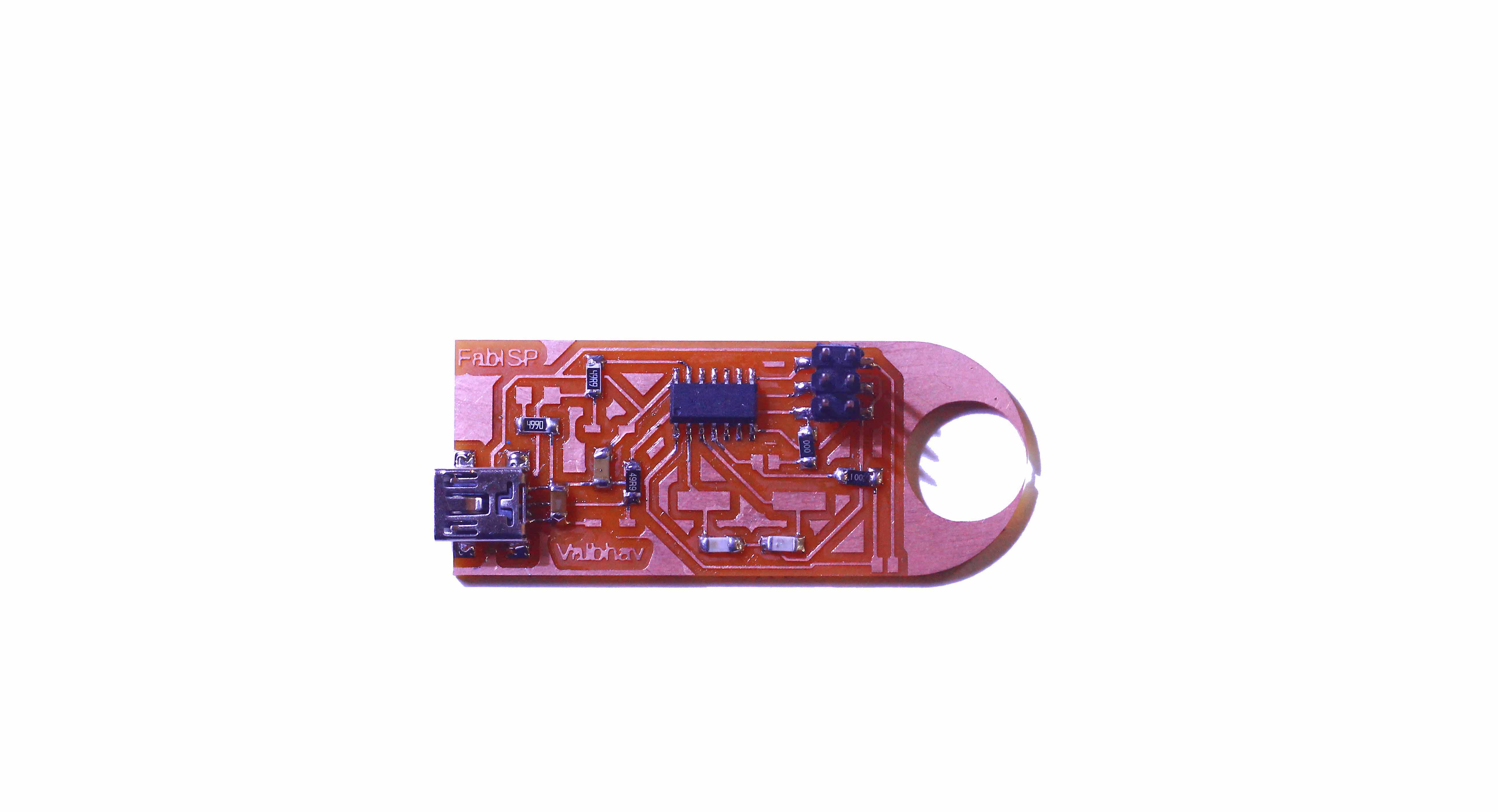
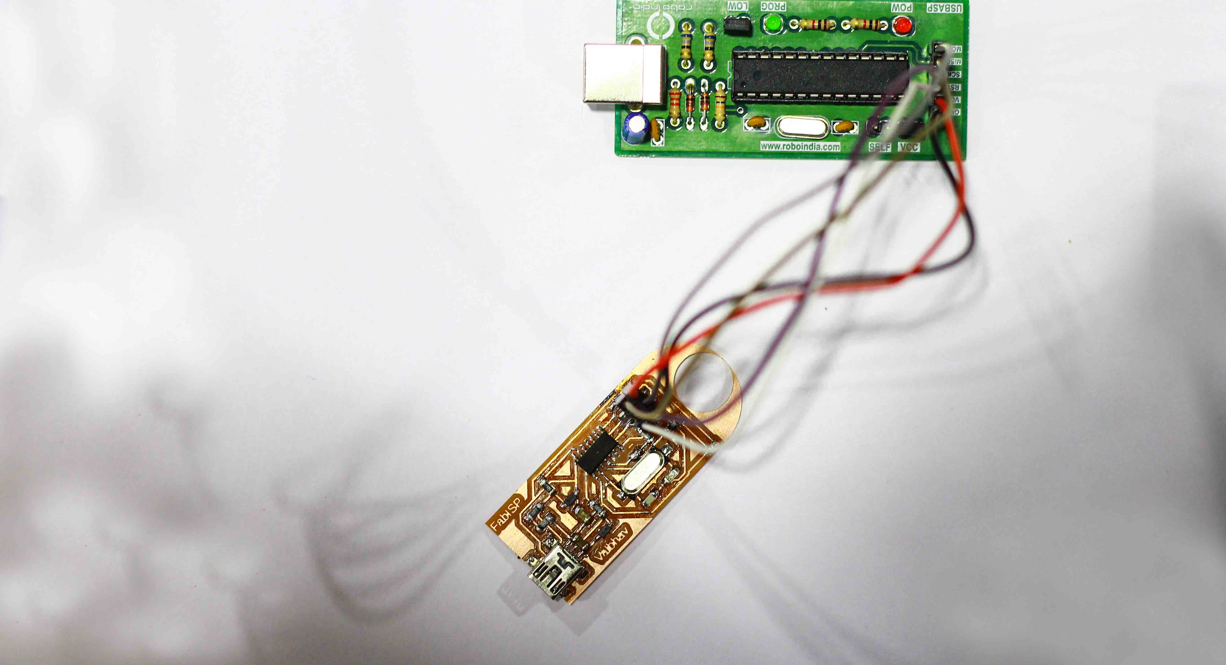
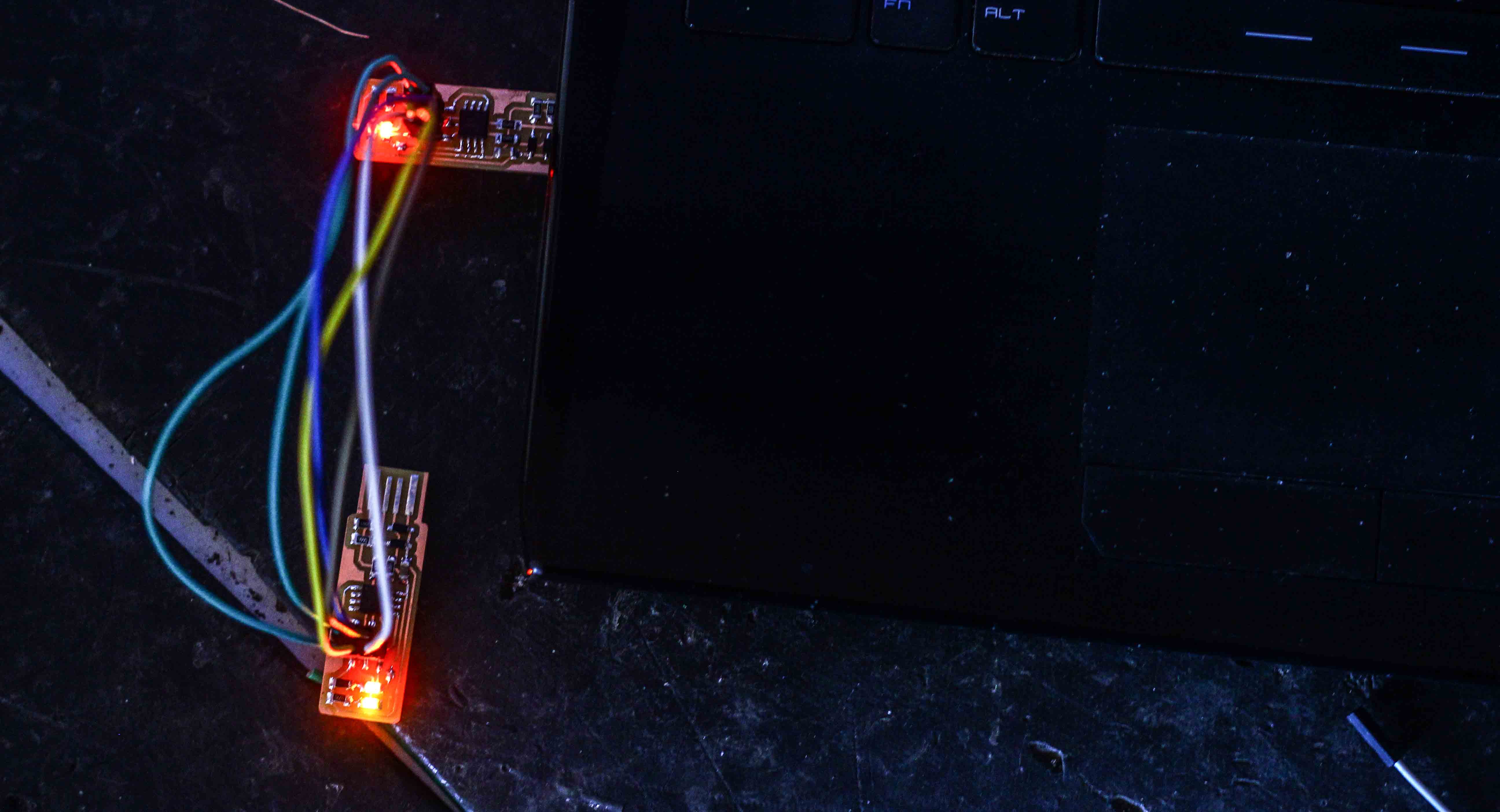
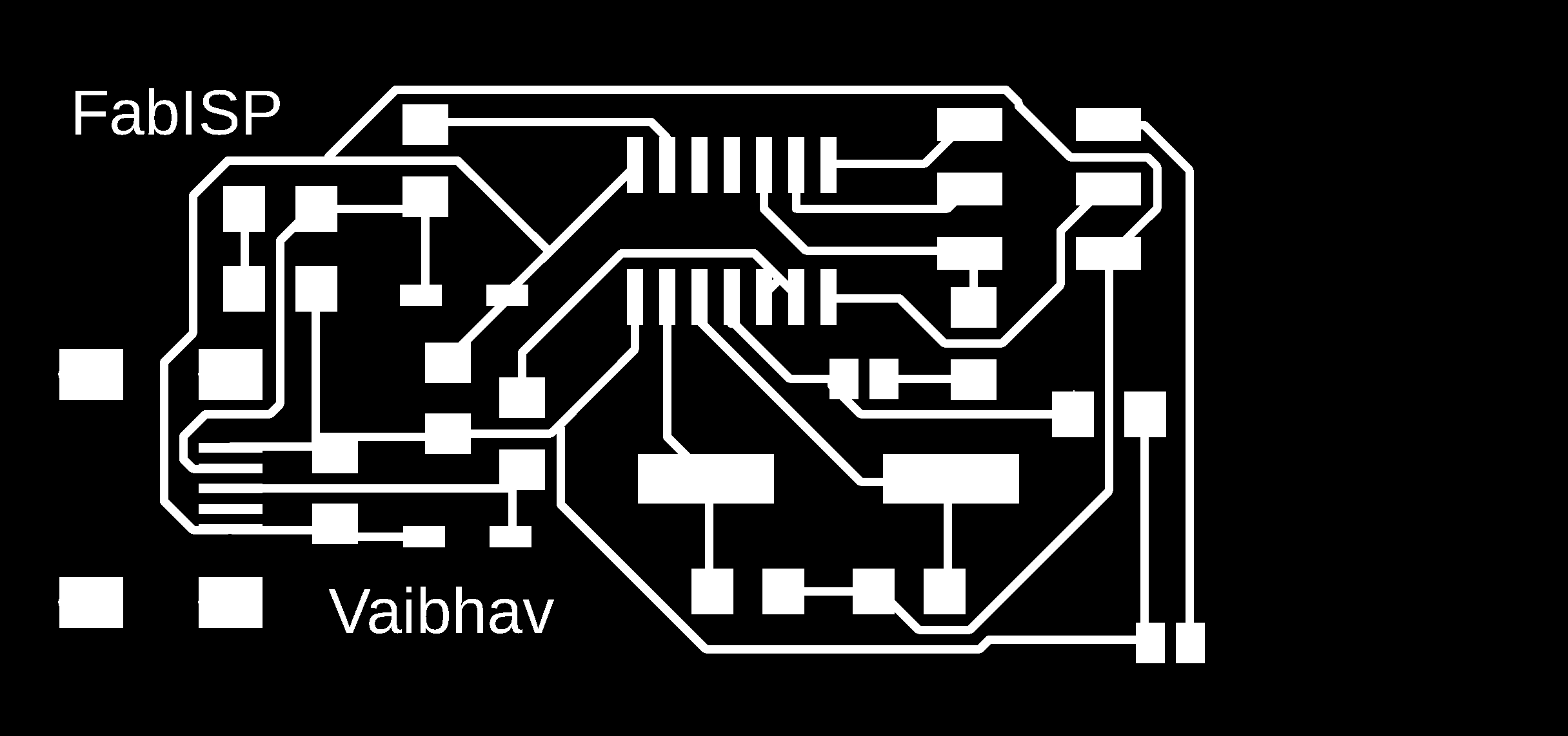
I have been looking forward to this week to start improving on my electronics section but also had this question when I started this week that why not design the board before going ahead with fabrication/milling(still have this question actually). But as it appeared I have to start with fabrication of a PCB before actually designing one. I used David's board since it was not documented properly and I thought of documenting it as good as possible. David's board also had lot of issues that I felt were addressed in later boards. It lacked LED and hence wasn't able to display whether the board was connected to the computer or not. Another drawback that I felt was connecting and disconnecting the solder jumpers once the programming is done, somehow I felt this made the process a bit cumbersome. My first board got programmed but didn't get detected even after several attempts, hence I decided to go with Brian's board(the second board got successful).
Group Assignment(including Line test)
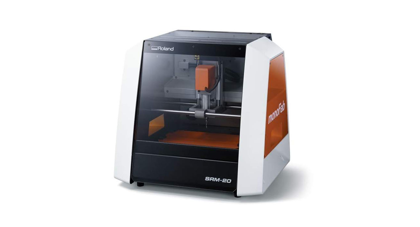
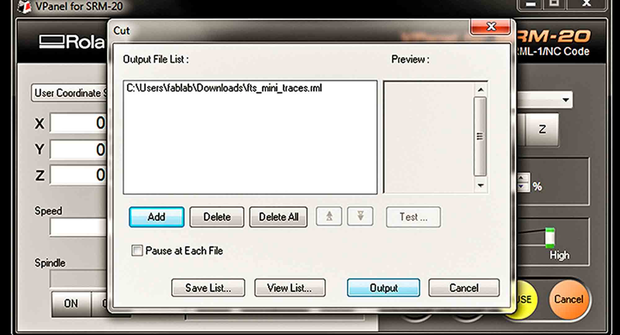
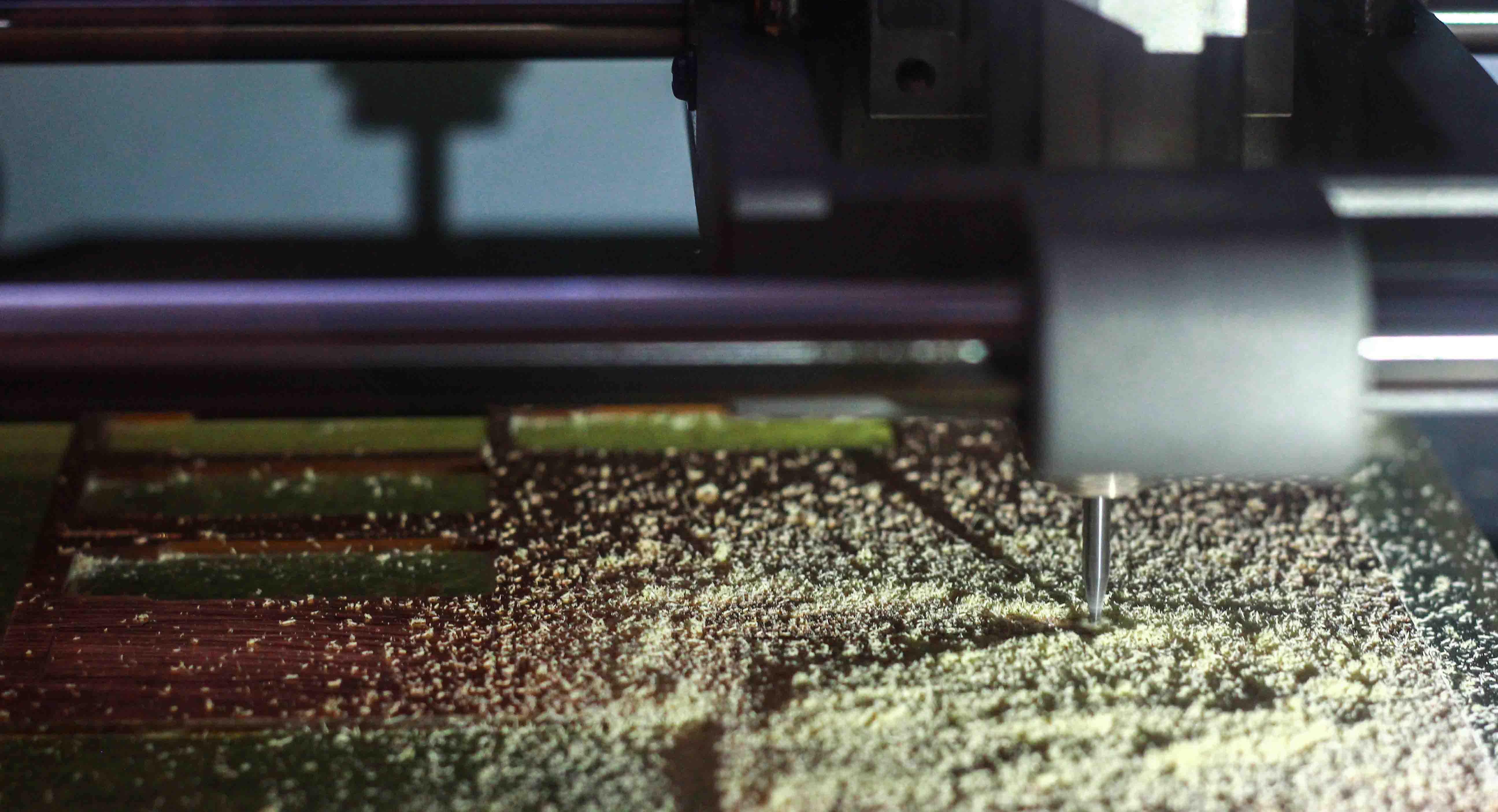
Although there are two PCB milling machines at our Fab Lab Roland Modela MDX-20 and Roland monoFab SRM 20, we preferred the latter one. The technical specifications for the machine can be found out here. To use the machine we followed the following steps:
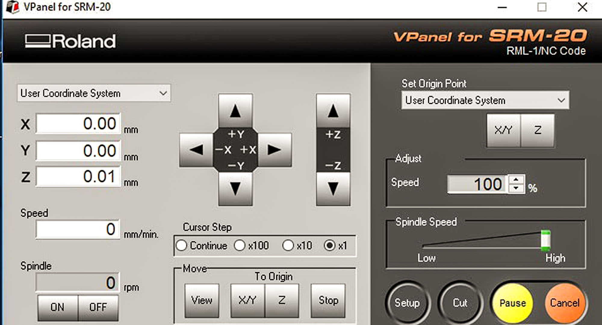
1. Levelling the bed and setting the origin: We used FR1 board for milling. The board is stuck to the bed using a double sided tape. Next we move the machine along X, Y and Z axis using the controls given on my SRM-20's software, to set the origin.
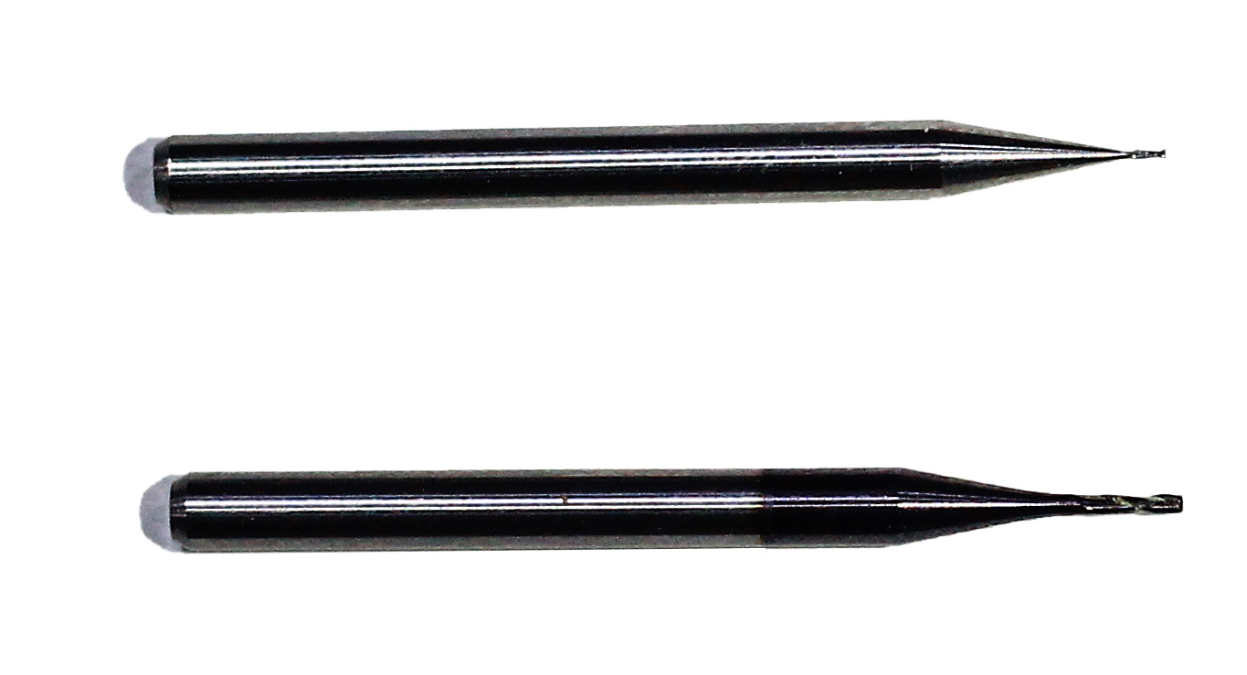
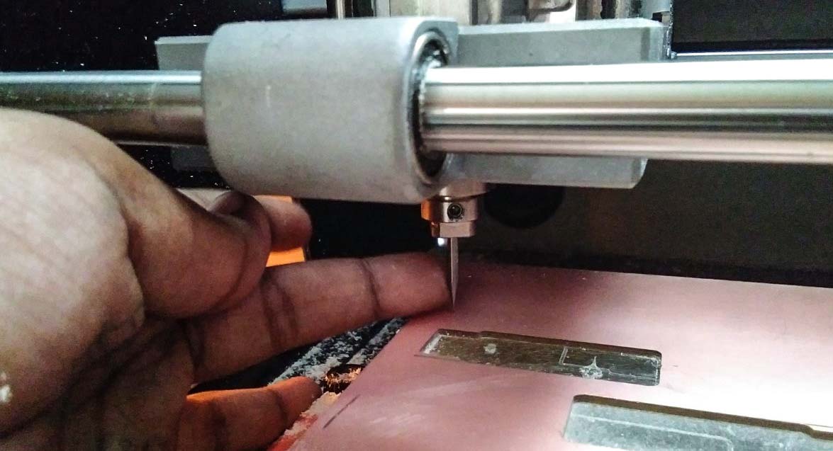
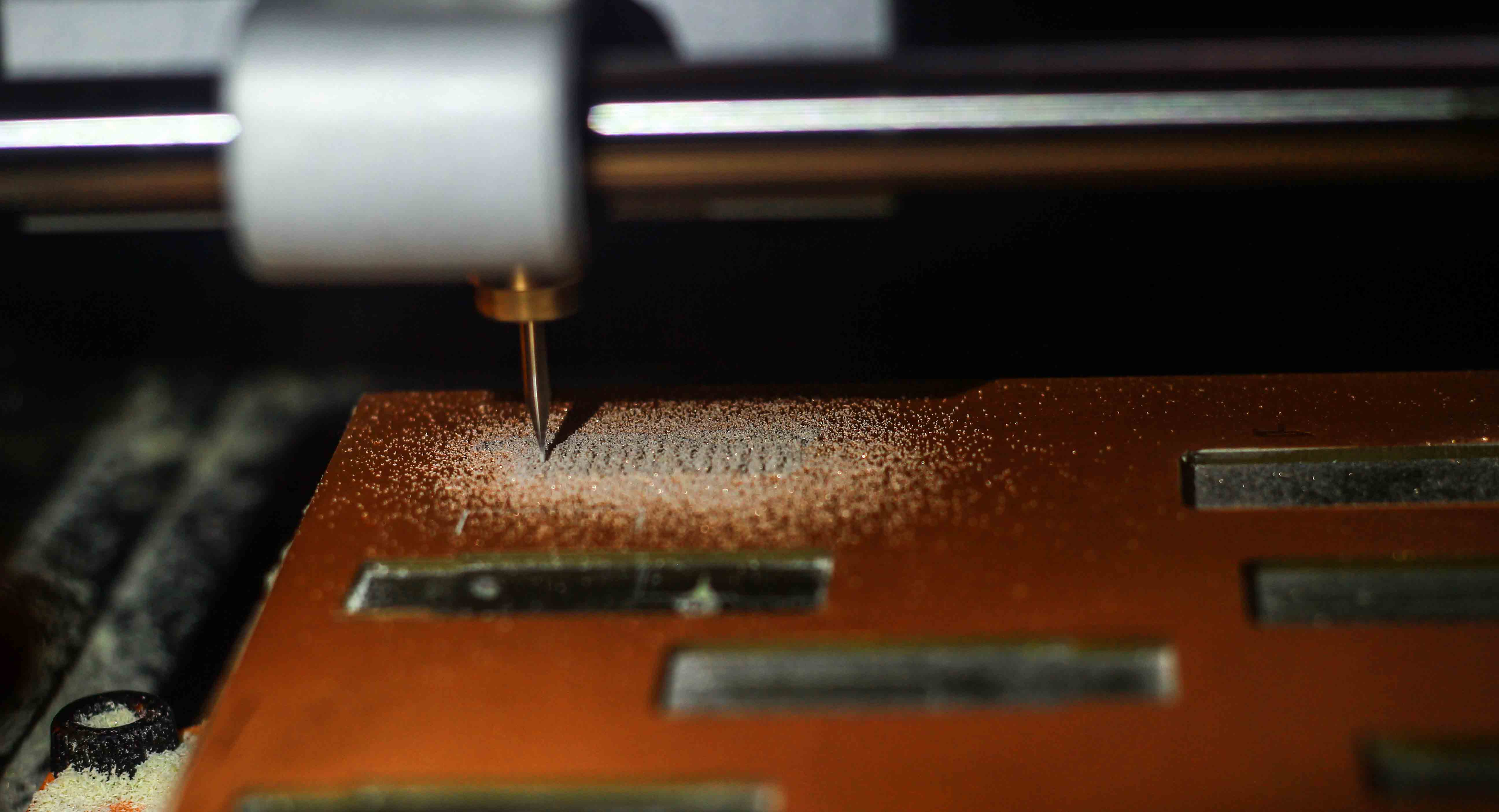
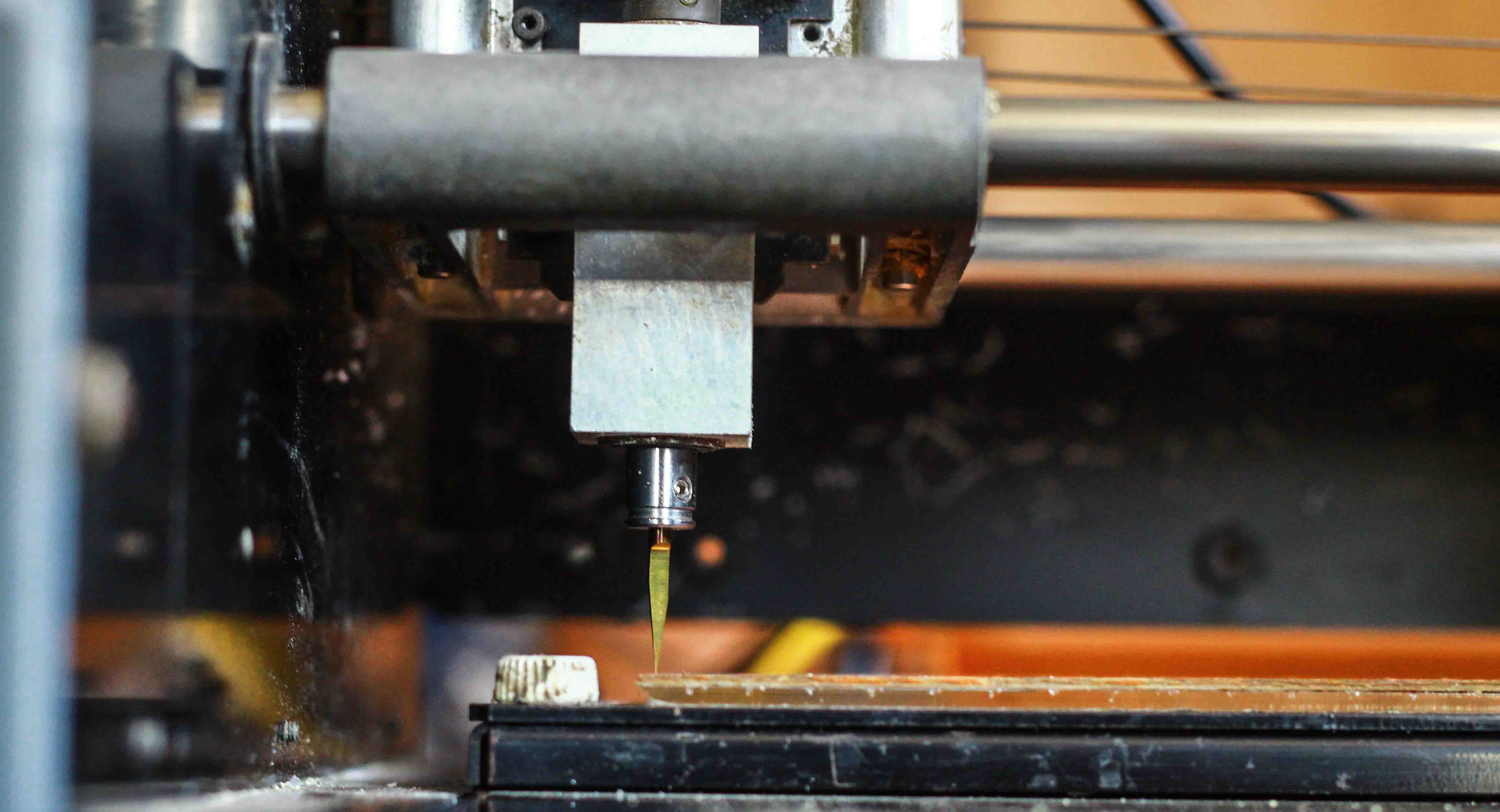
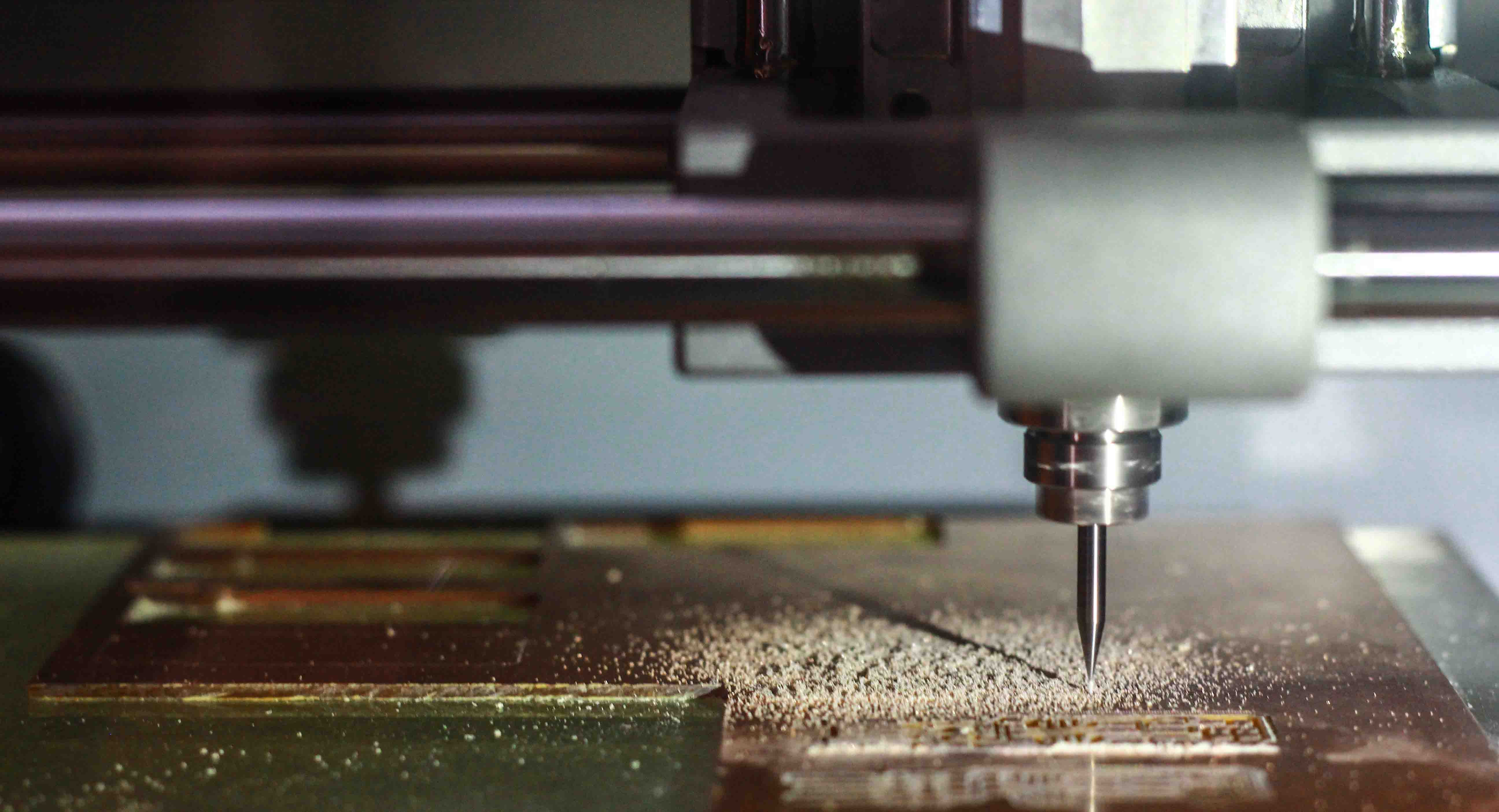
2. Using the end mills: A word of caution here, 1/64 inch and 1/32 inch end mills are very small and there are good chances that they can break if mishandled or aren't fitted properly. A dry run is always beneficial before actual milling. It involves setting the "Z" above the board level, so that machine will just hover giving you an idea about the actual extent of milling. First we mill the traces using 1/64 inch end mill and then we use 1/32 inch end mill to cut the boundaries of the board in order to remove it.
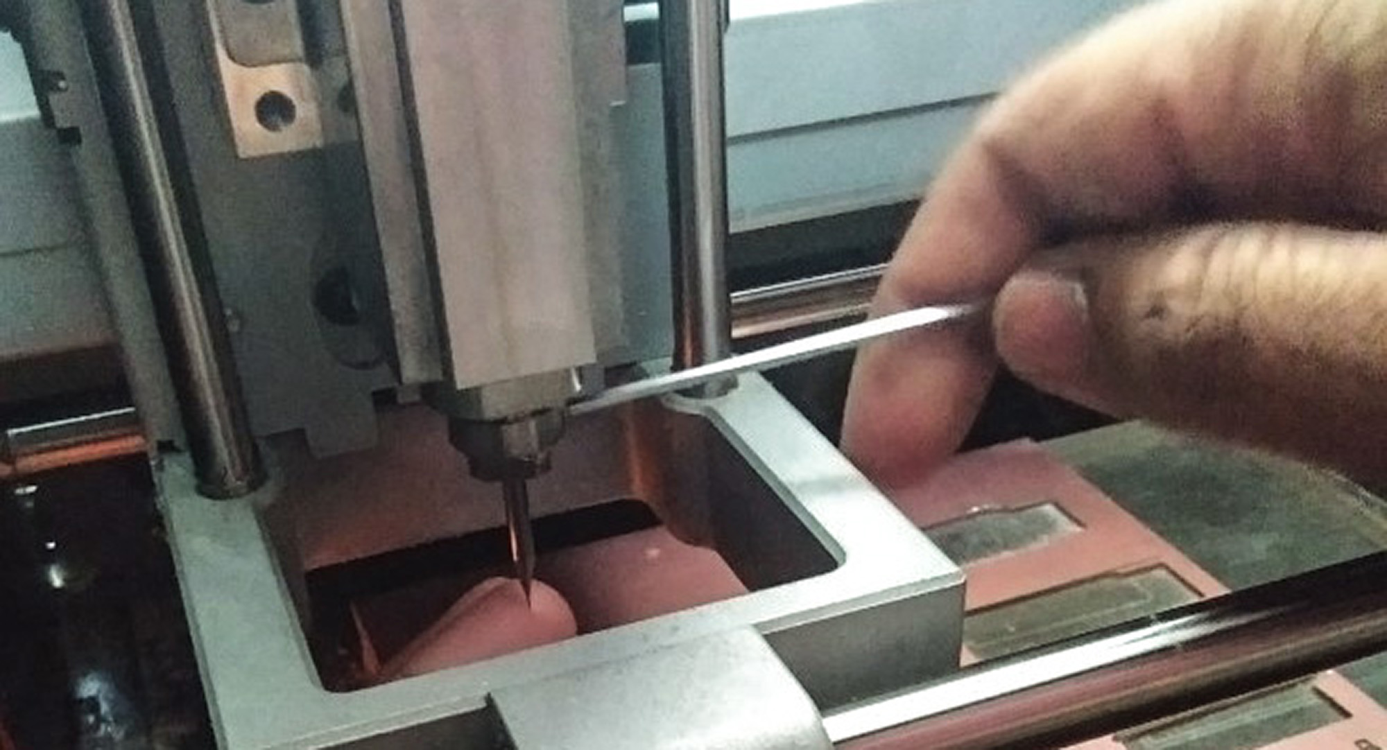
3. Using gravity to set the end mill: Try to bring Z as close(5 mm) as possible to the milling board and then losen the collet a little bit and drop the end mill. Then set Z as zero in the dialog box.
One of the major drawbacks of the machine that we found out is the absence of artificial lighting inside the machine.
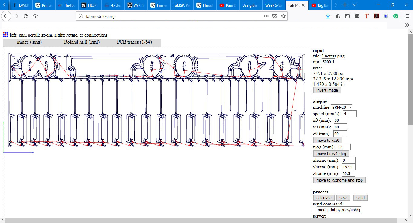
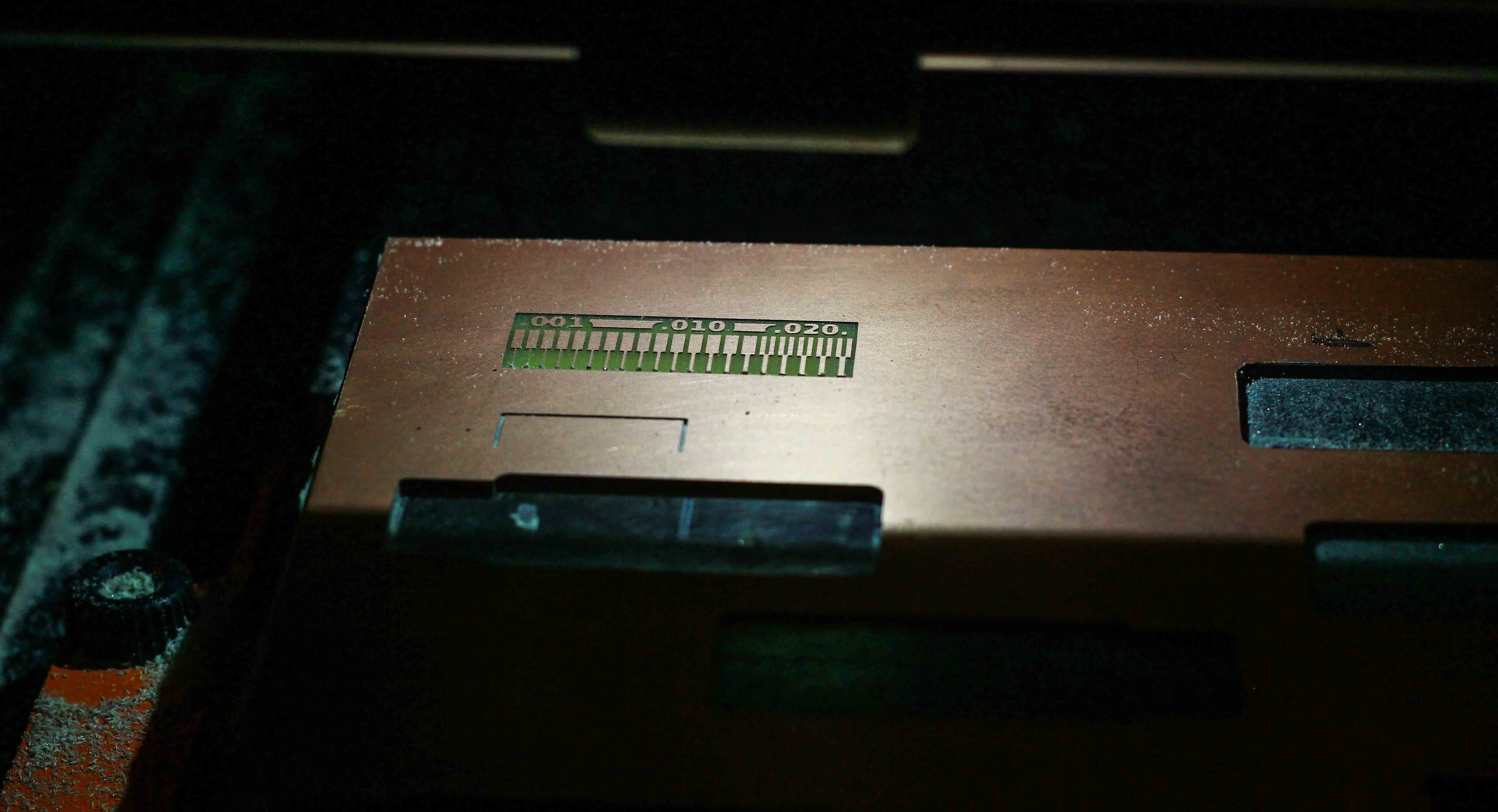
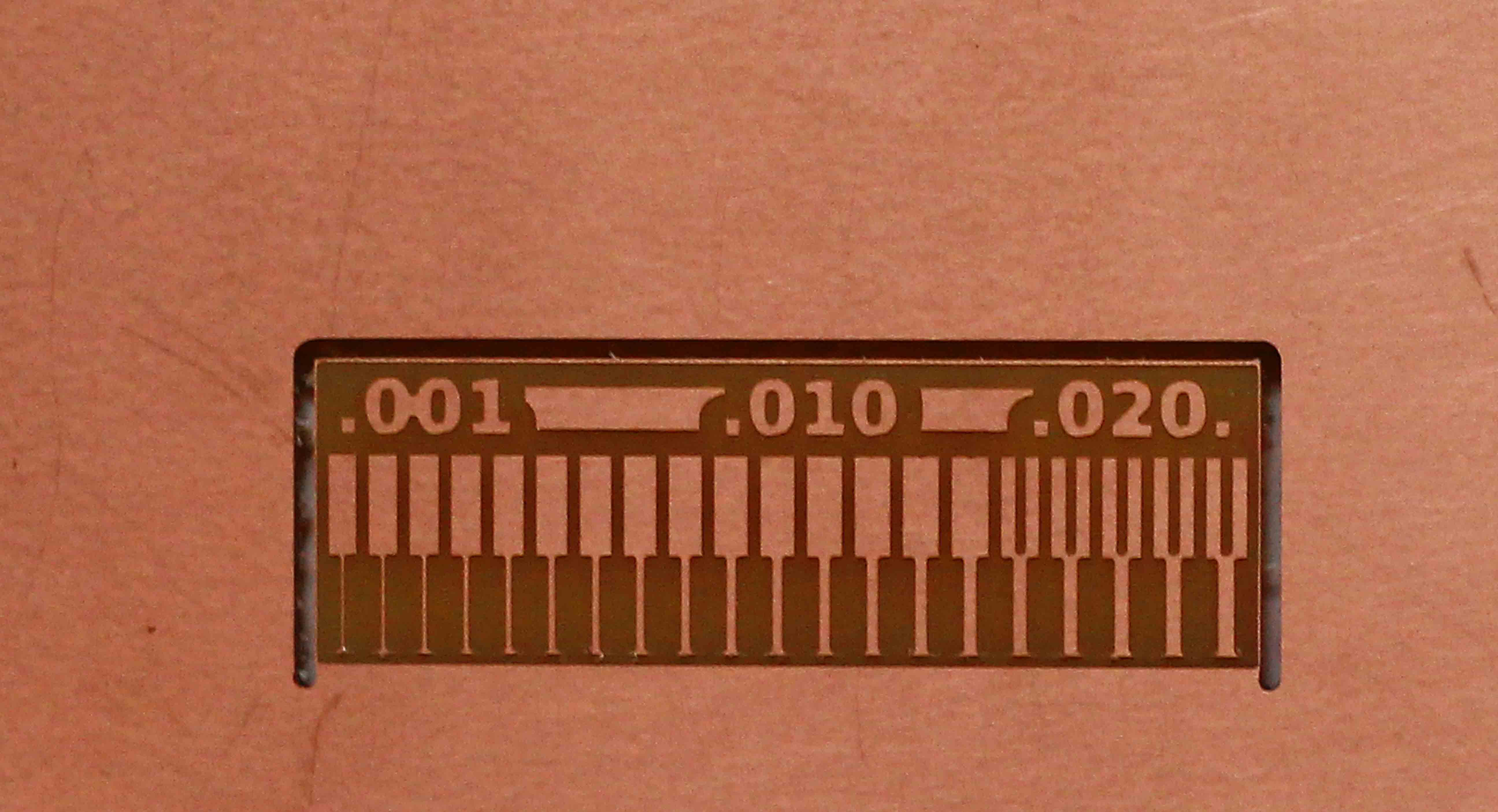
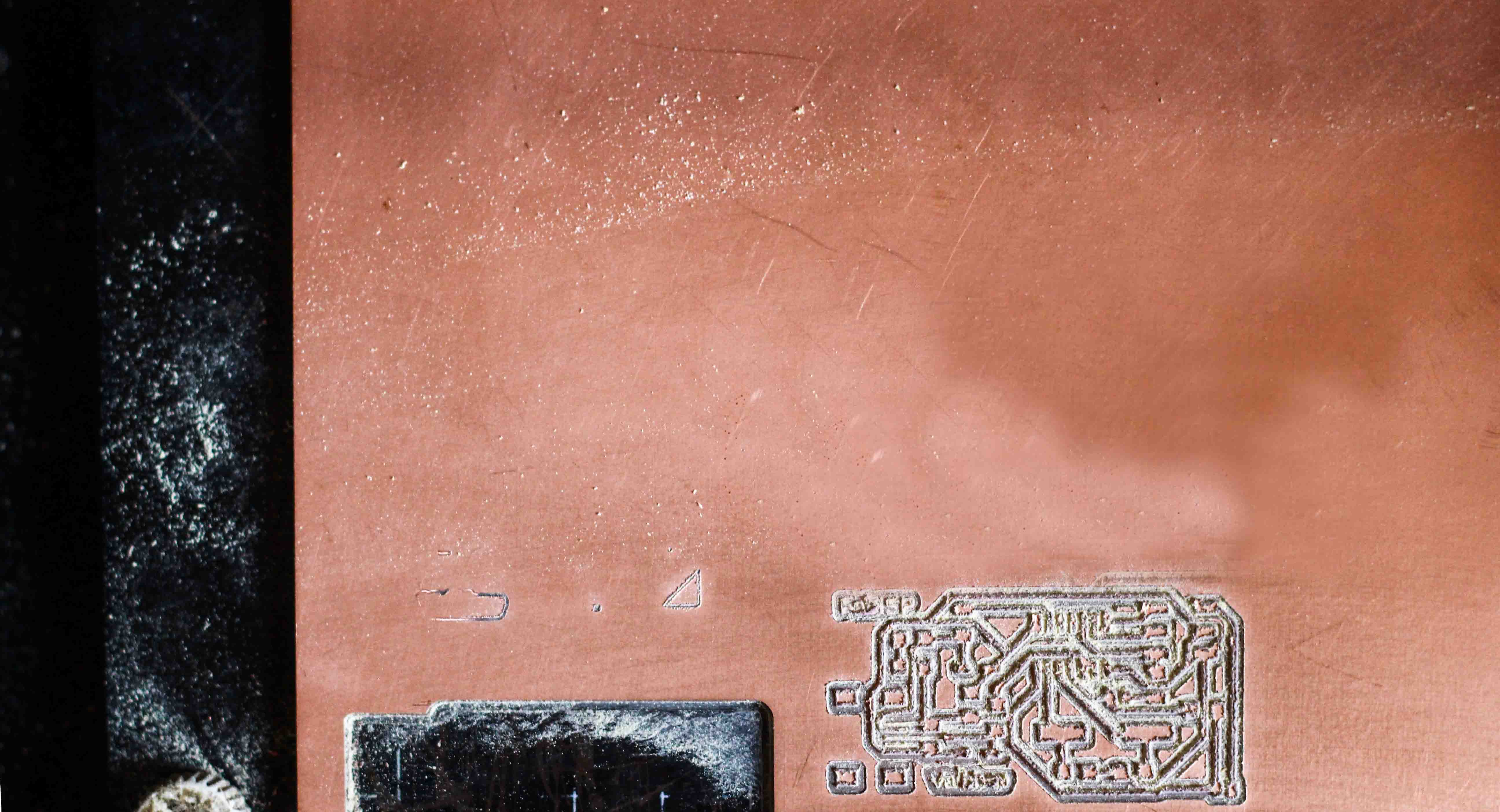
It is important to do a "line test" (kind of based on similar lines like that of comb test) before actually milling a PCB. So what is a line test, line test is basically used to see how fine a track can be milled by a particular end mill. I used 1/64 inch end mill on a Roland monofab SRM20 to mill a design already available online and here. The line test has lines of varying thickness starting from 0.02 inch(0.508 mm) down to 0.001 inch(0.0254 mm). Neil showed us a photograph of a milled line test and the thinnest one didn't mill properly. In my case, even the thinnest line of 0.001 inch came out clearly and precisely. The only reason I can think of is the difference between the machines. This line test will help us in electronics design as to how thin your trace can be and still be easily milled by the milling machine.
Generating file and milling
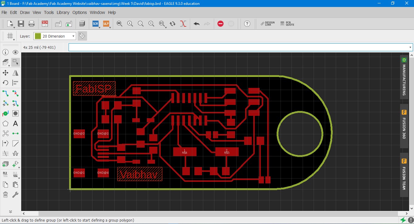
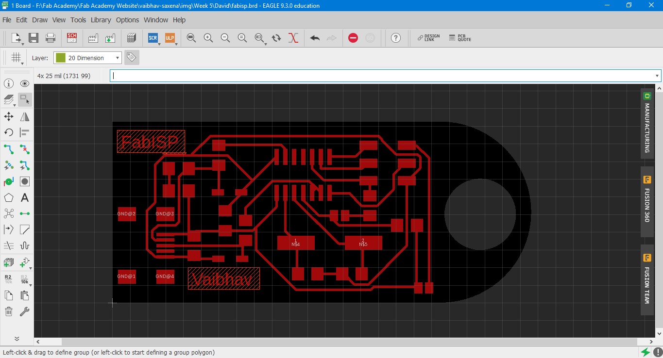
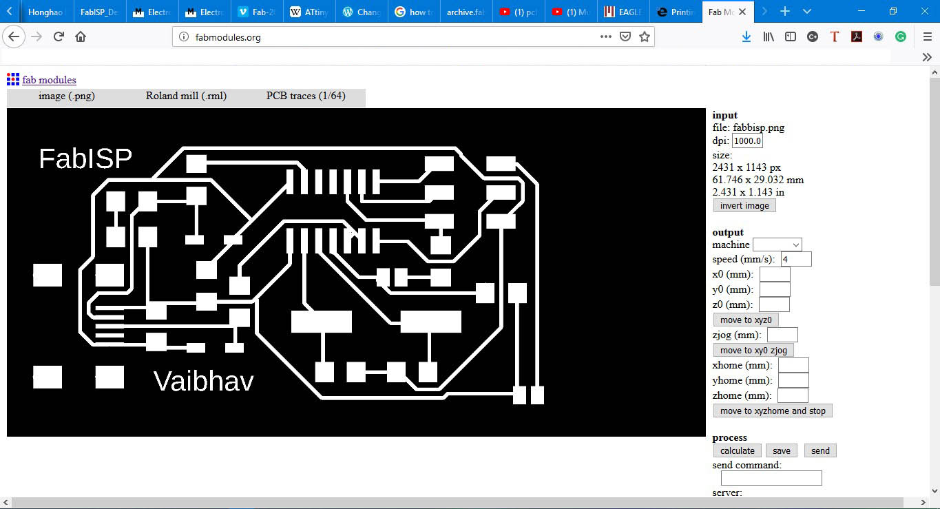
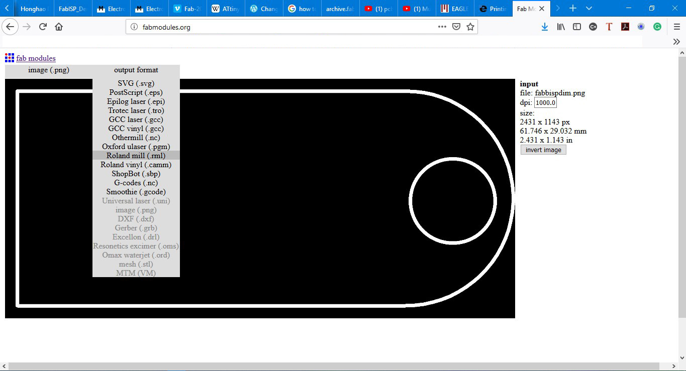
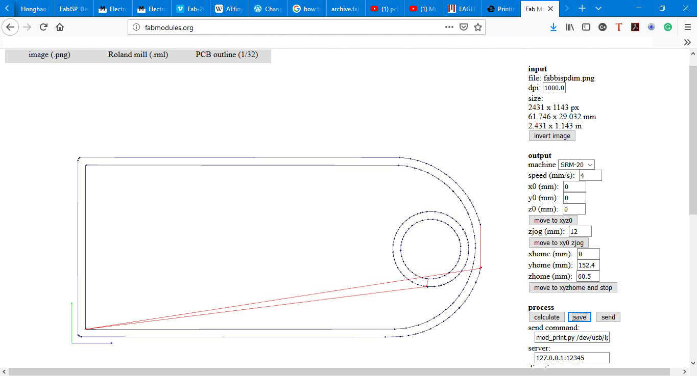
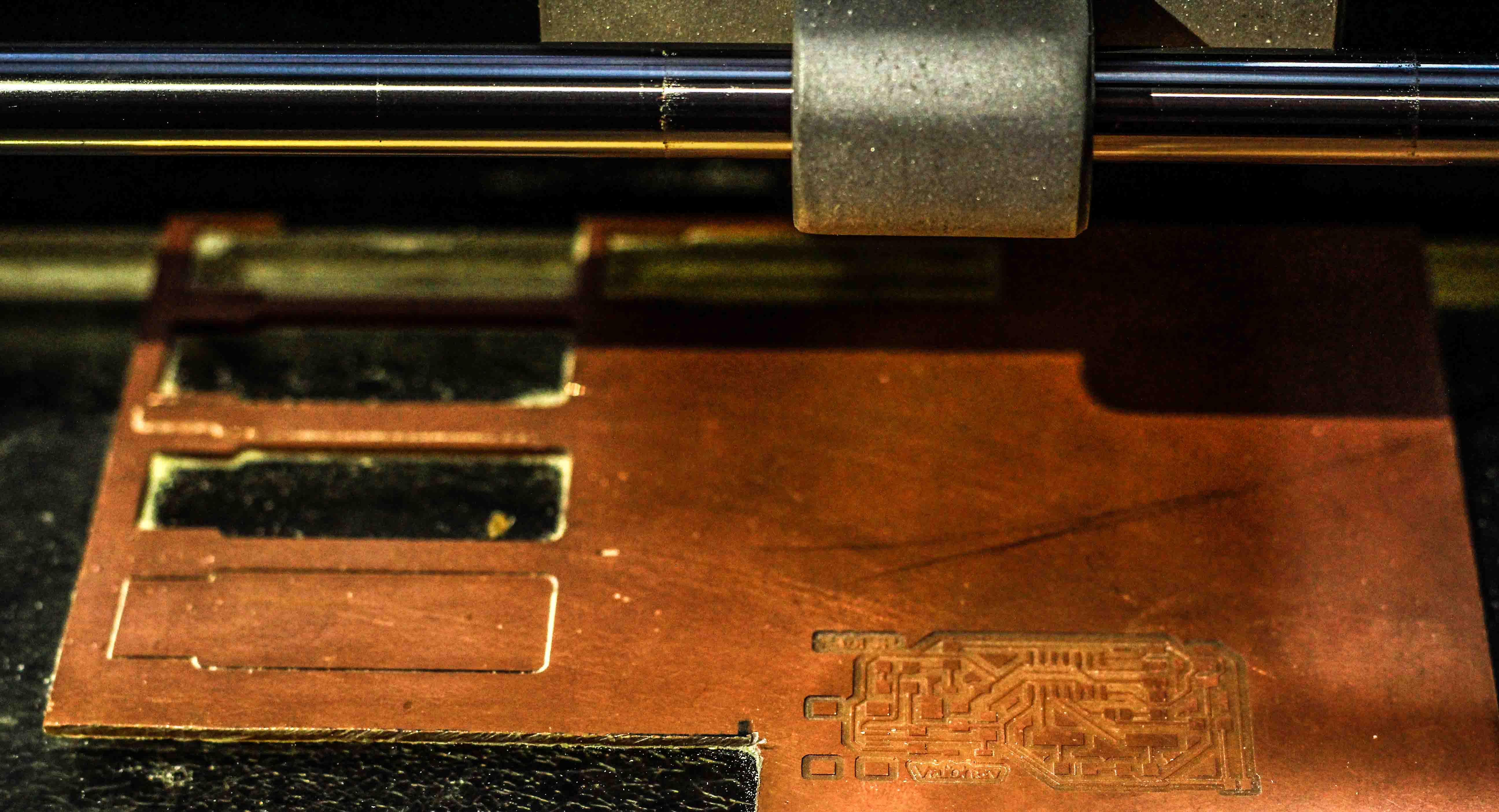
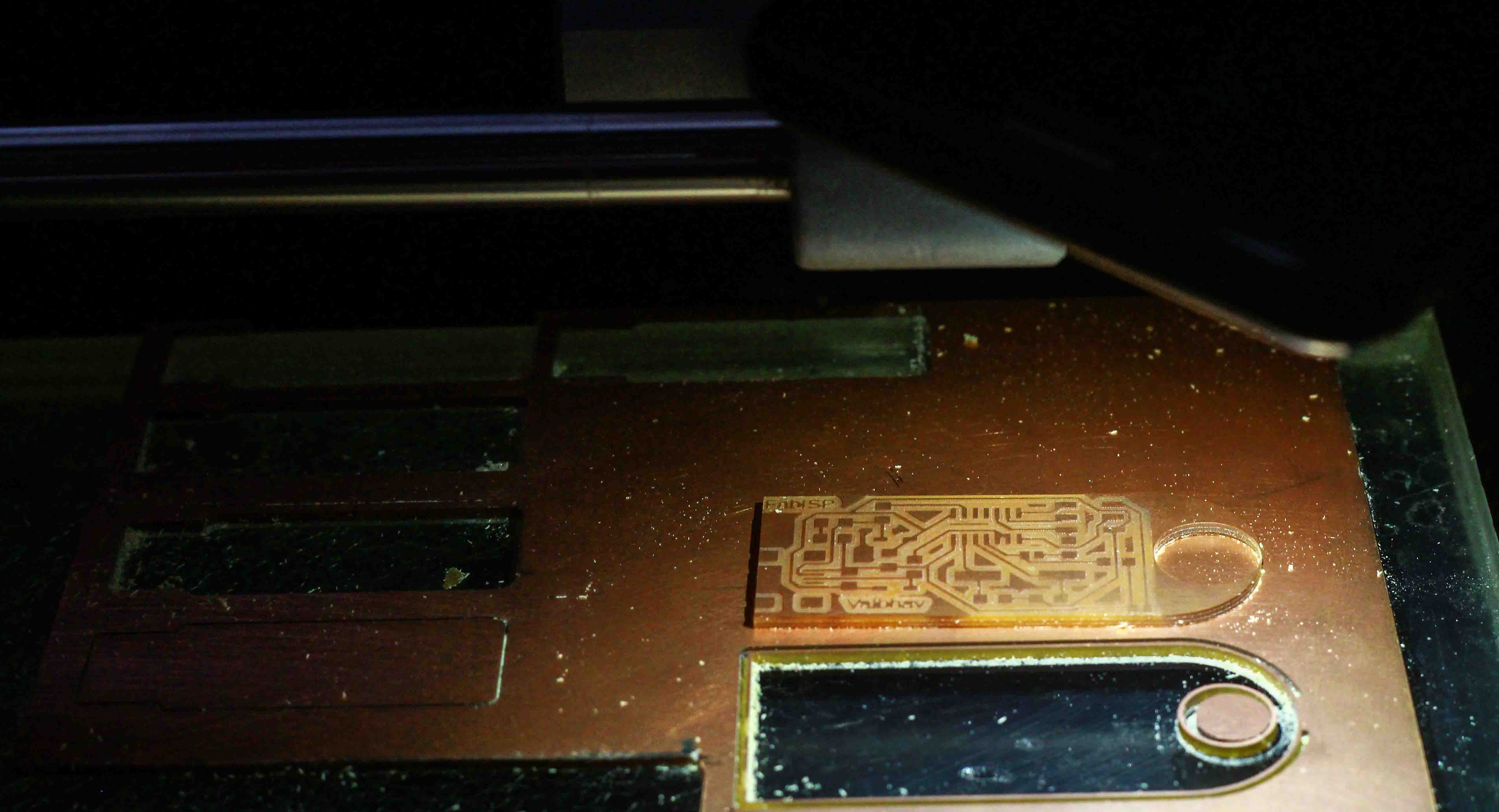
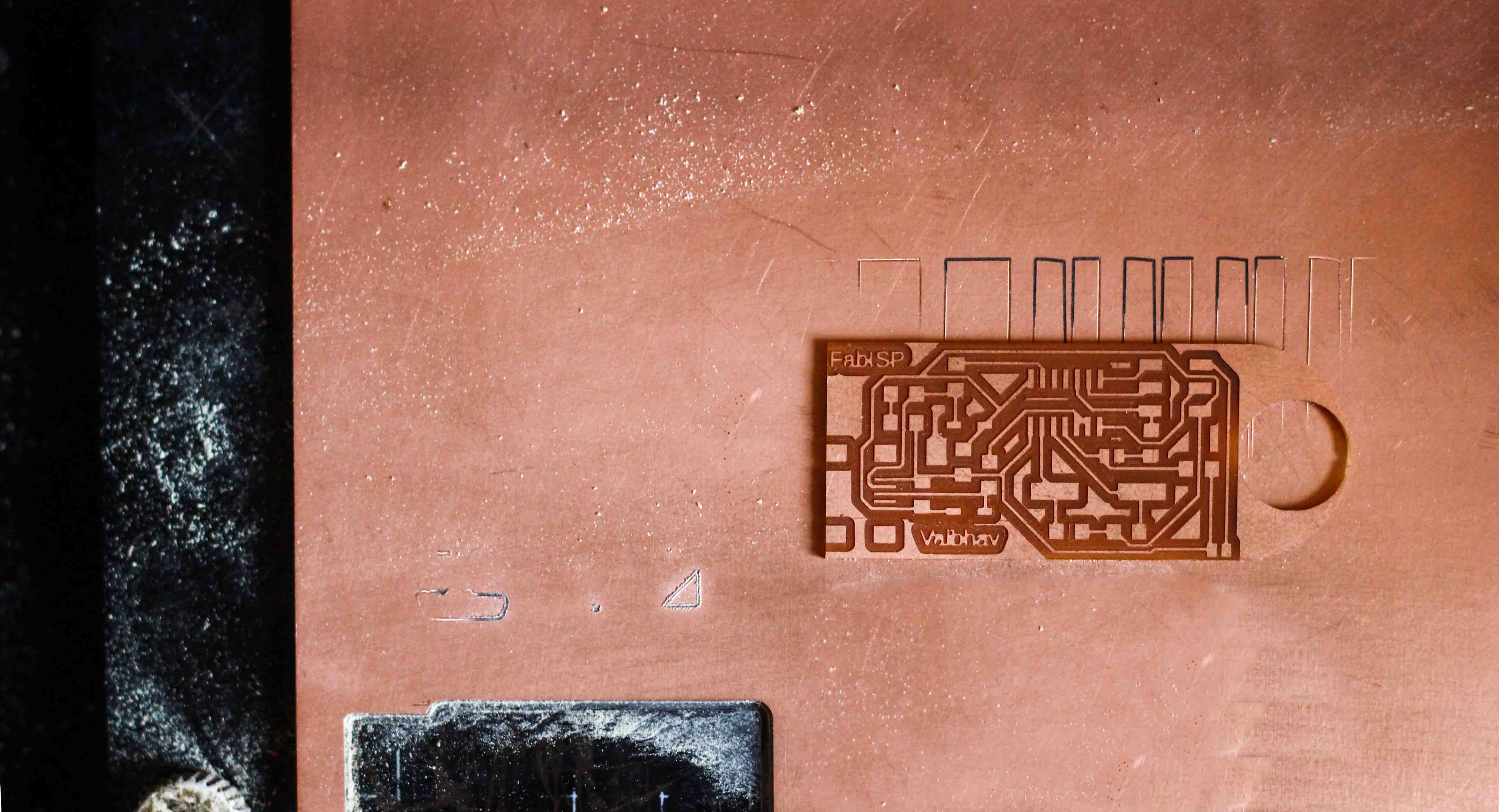
I started with downloading the .brd file of David's board. I made some modifications to David's design by changing the shape of the PCB to a dog tag and adding my name in Autodesk Eagle. I then exported the file to .png format. I used fabmodules to generate the .rml file for interior and exterior traces. I used 1/64 inch milling bit for interior and 1/32 for exterior traces.
While milling my first PCB, I tried to do it using Roland Modela MDX-20 but quickly realized that the bit was broken and immediately aborted PCB milling. There is a difference between the bit structure of Modela MDX-20(V milling bits, it kept on breaking) and SRM 20. One of the disadvantages both these machines have is the bed levelling which kept on breaking the milling bits. I ultimately used Roland monoFab SRM 20 to mill my PCB on FR-1.
Steps to follow before milling:
1. Add a sacrificial layer on the milling bed.
2. Prevent any air bubbles while sticking the PCB.
3. Place the milling bit on the bed using gravity(don't drop it) and place is preferably on a higher level, if the bed is slightly uneven.
Everything looked fine except for the traces of my name "Vaibhav" and "FabISP" that didn't come out properly, since it was too thin for 1/64 inch milling bit. Another issue that I realized was with fab modules while generating .rml file. The interior was perfectly fine but while I was generating .rml file for cutting the PCB it was showing two paths, one outside and one inside the actual trace line.
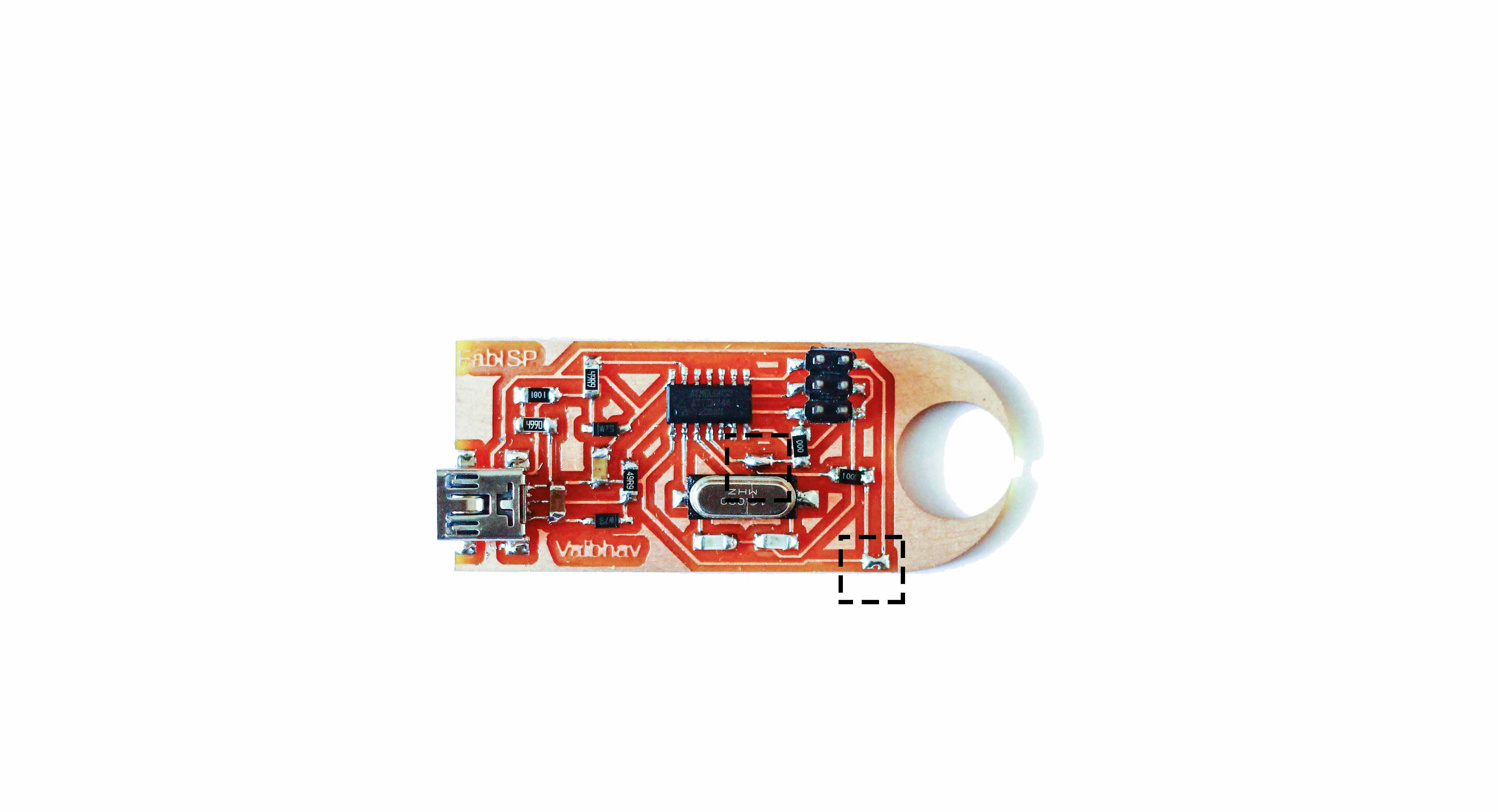
Also one important thing to note of importance is that the solder jumpers when connected make the FabISP vulnerable to be reprogrammed, only when one of them is disconnected it cannot be reporgrammed, hence after it is programmed SJ1 should be disconnected.
Soldering
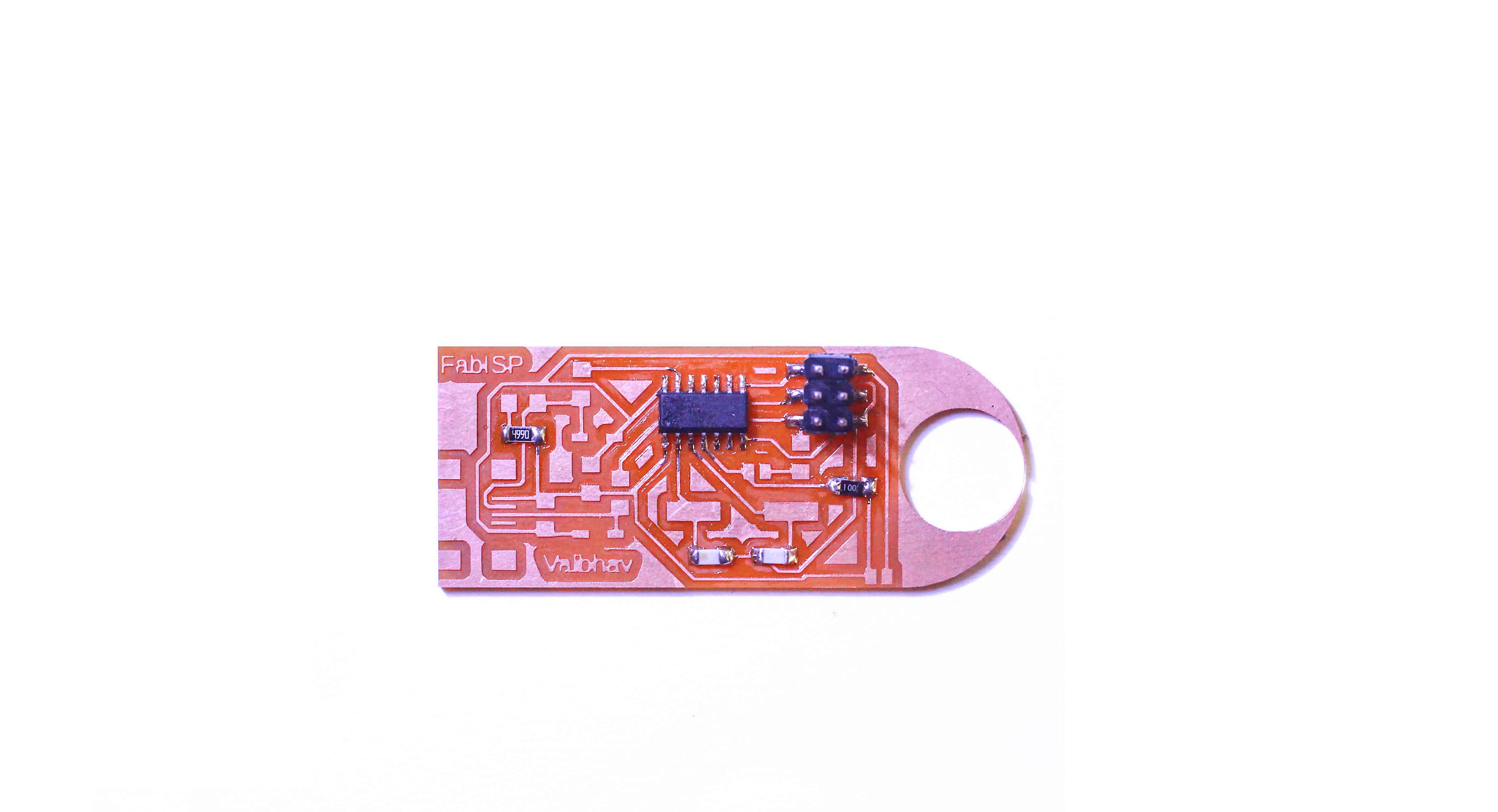
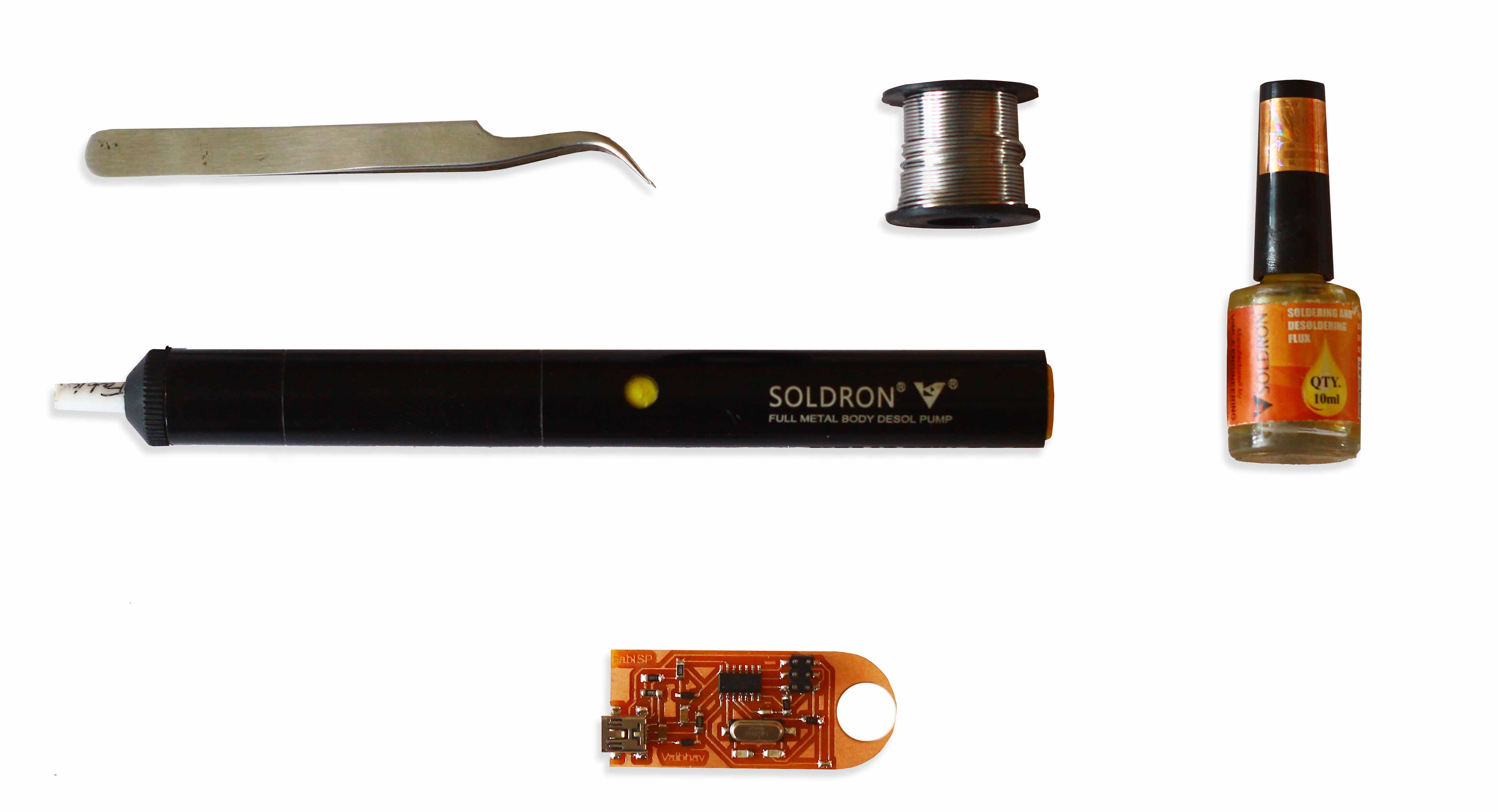
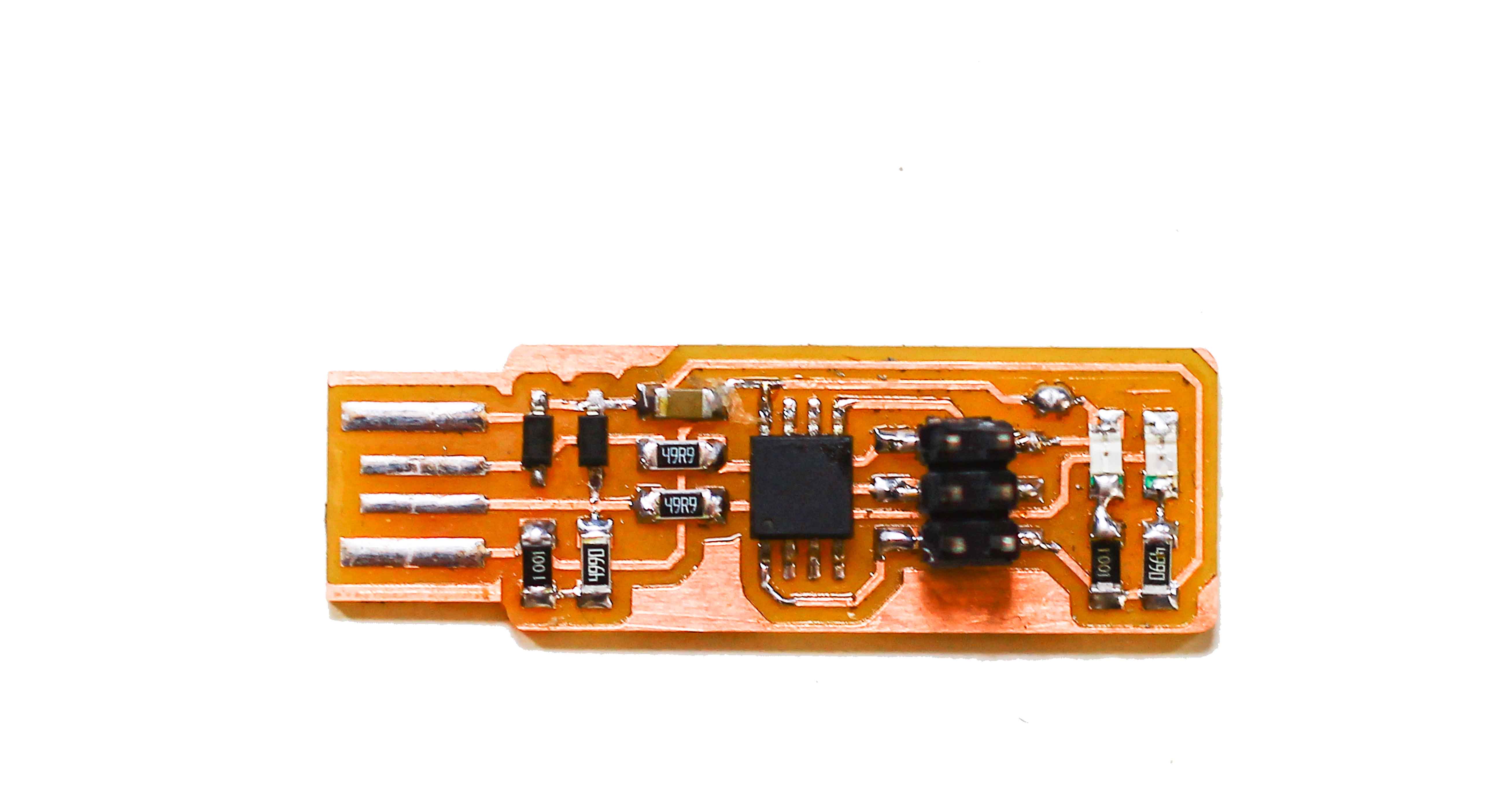
The components(BOM) for the FabISP are listed below:
1. ATtiny 44 x1 (The circle should be identified before soldering the microcontroller)
2. Zener Diode 3.3v x2 (the black line denotes positive side)
3. Crystal 16 MHz x1 (instead of 12MHz used by David)
4. 1000 Ohm Resistor x1 (identified as 1002)
5. 1000 Ohm Resistor x1 (identified as 1001)
6. 499 Ohm Resistor x1 (identified as 4990)
7. 49 Ohm Resistor x2 (identified as 49R9)
8. 0 Ohm Resistor x1 (identified as 000)
9. 22 PicoFarad Capacitor x2
10. 0.1 MicroFarad Capacitor x1
11. 10 MicroFarad Capacitor x1
12. Mini-B USB Connector x1
13. 6 Pin Header x1
Things to do before soldering:
1. Rub the surface of the freshly milled PCB board with a higher grit sandpaper.
2. Clean the tip of soldering iron.
3. I heated my soldering iron to 340° C before using it.
4. Apply flux to the trace pads before soldering.
5. The technique that worked: I applied very little solder to one of the pads that acted as glue for the component. I then held the component with a tweezer in one hand and soldering iron in another, heated the pad containing solder a bit and placed the component immediately. The component is slightly fixed now and now other pad can be easily soldered.
Programming ISP
David mentioned to use WinAVR(to install the development tools for AVR microcontrollers) but since it hasn't been maintained for years and isn't good for Windows 10 hence, I went with the following to program FabISP and they are as follows(based on Brian's documentation). I used USBasp as a programmer to program my FabISP:
1. Download and unzip David's firmware : The firmware already contains a hex file that the FabISP can read
2. Install Git : used to execute commands from a specific folder, on the other hand command prompt could also be used to locate to the specific folder where firmware is located
3. Download and install Atmel GNU Toolchain: a collection of tools/libraries used to create applications for AVR® microcontrollers
4. Download and install GNU Make
5. Download and install avrdude
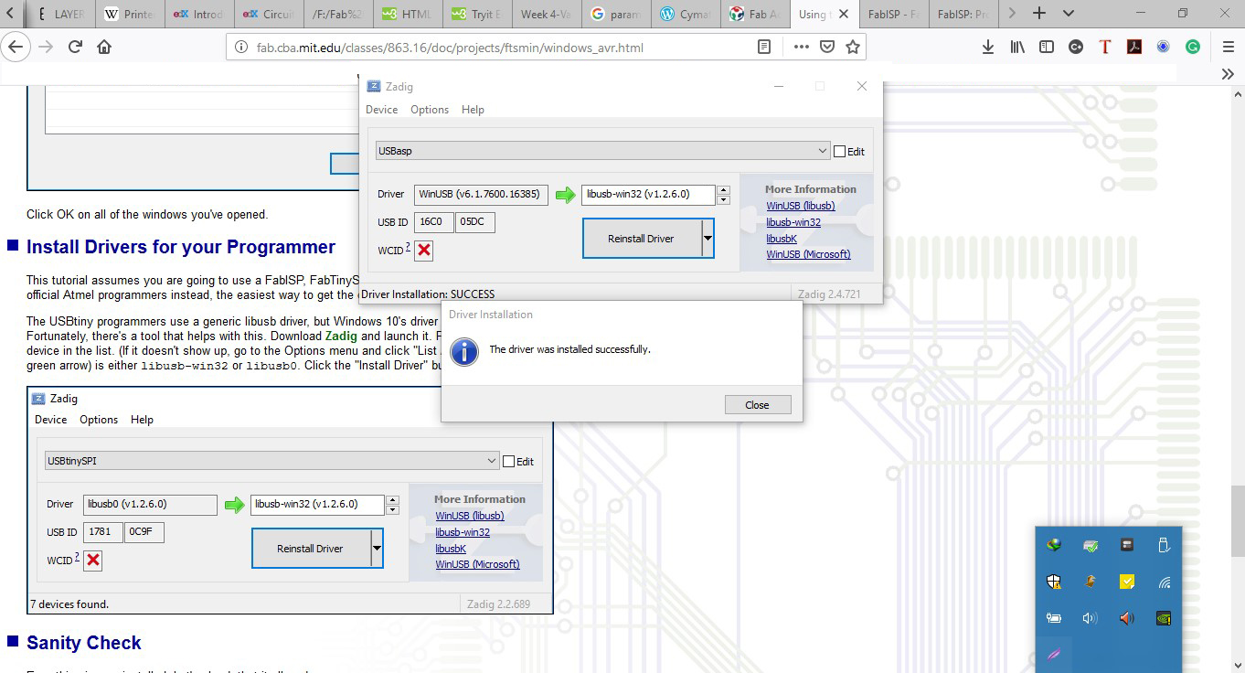
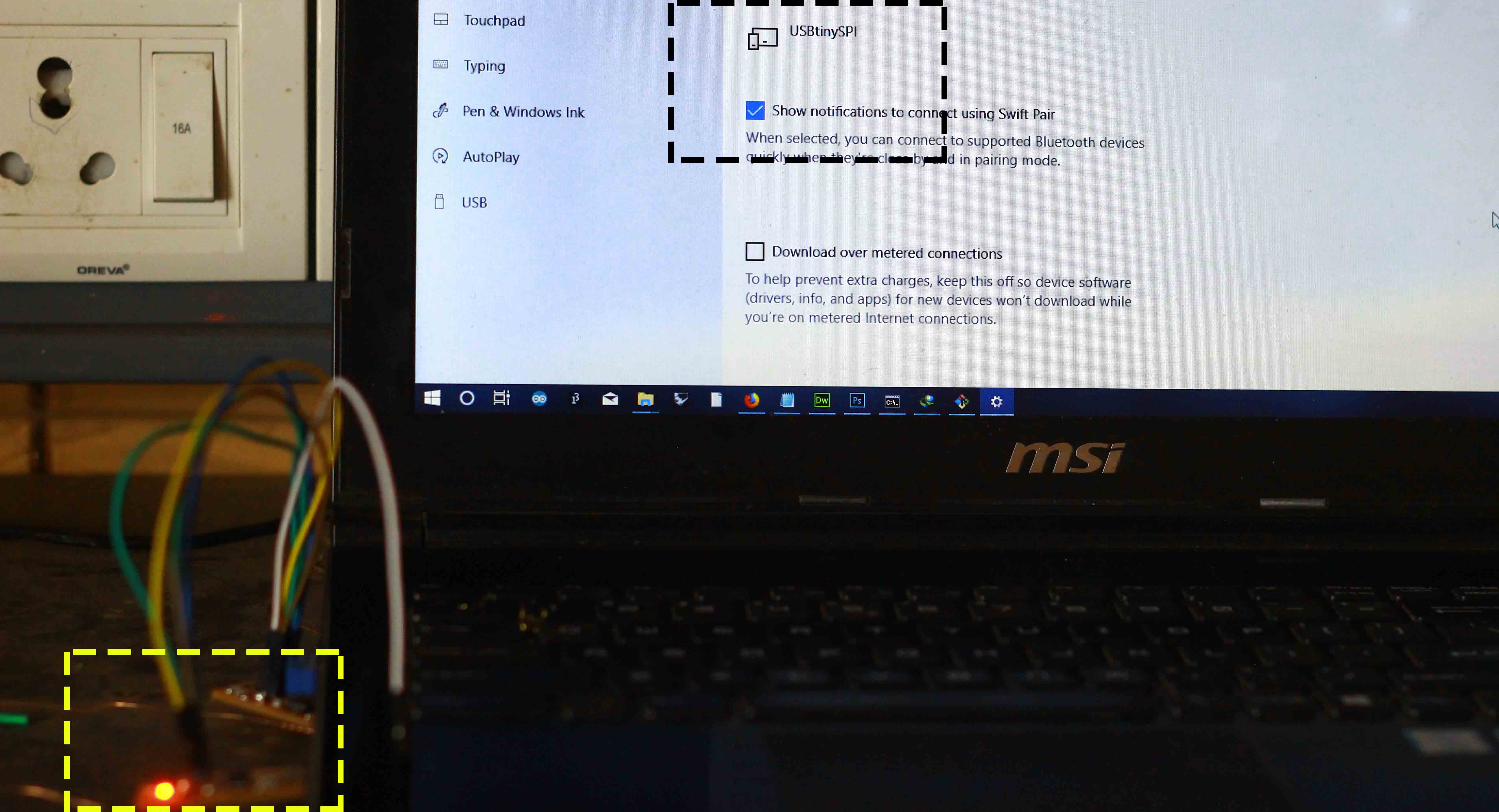
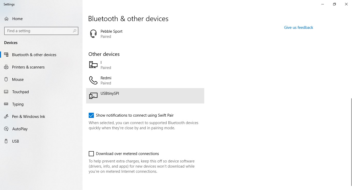
6. Download Zadig to install drivers for the programmer
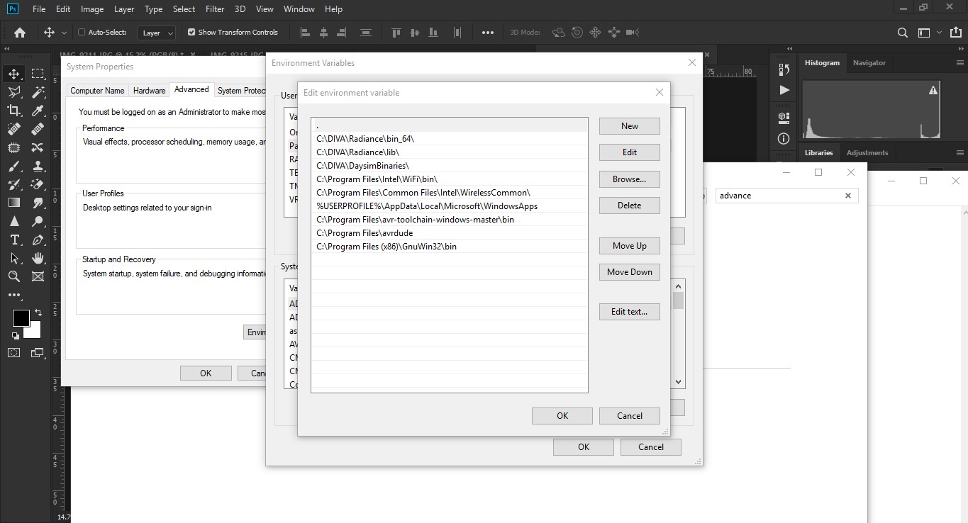
After installing all of the above, update the path by going to Start Menu>Control Panel>System. From left pane, choose Advanced System Settings and under Advanced tab go to "Environments Variables" (check the illustration above)
The three values to add are:
C:\Program Files\avr8-gnu-toolchain\bin
C:\Program Files (x86)\GnuWin32\bin
C:\Program Files\avrdude
Now we will install drivers for the programmer, we will use Zadig(mentioned above) to install the drivers for the programmer.(check the illustration above)
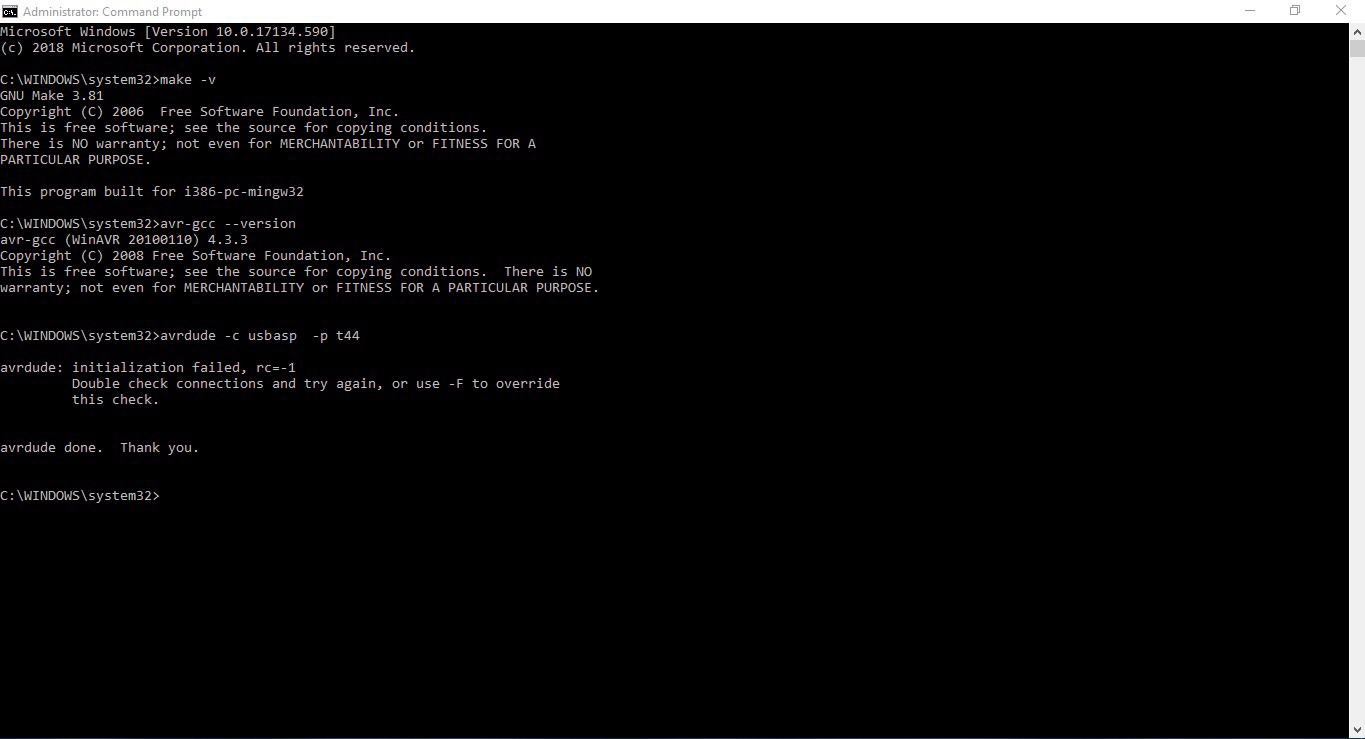
To check whether everything is installed, open command prompt as administrator and use these commands one after another:
1. make -v and press enter
2. avr-gcc --version and press enter
3. avrdude -c usbasp -p attiny44 and press enter
If the above commands provide the results as displayed in the illustration above then we are ready to proceed to the next steps.
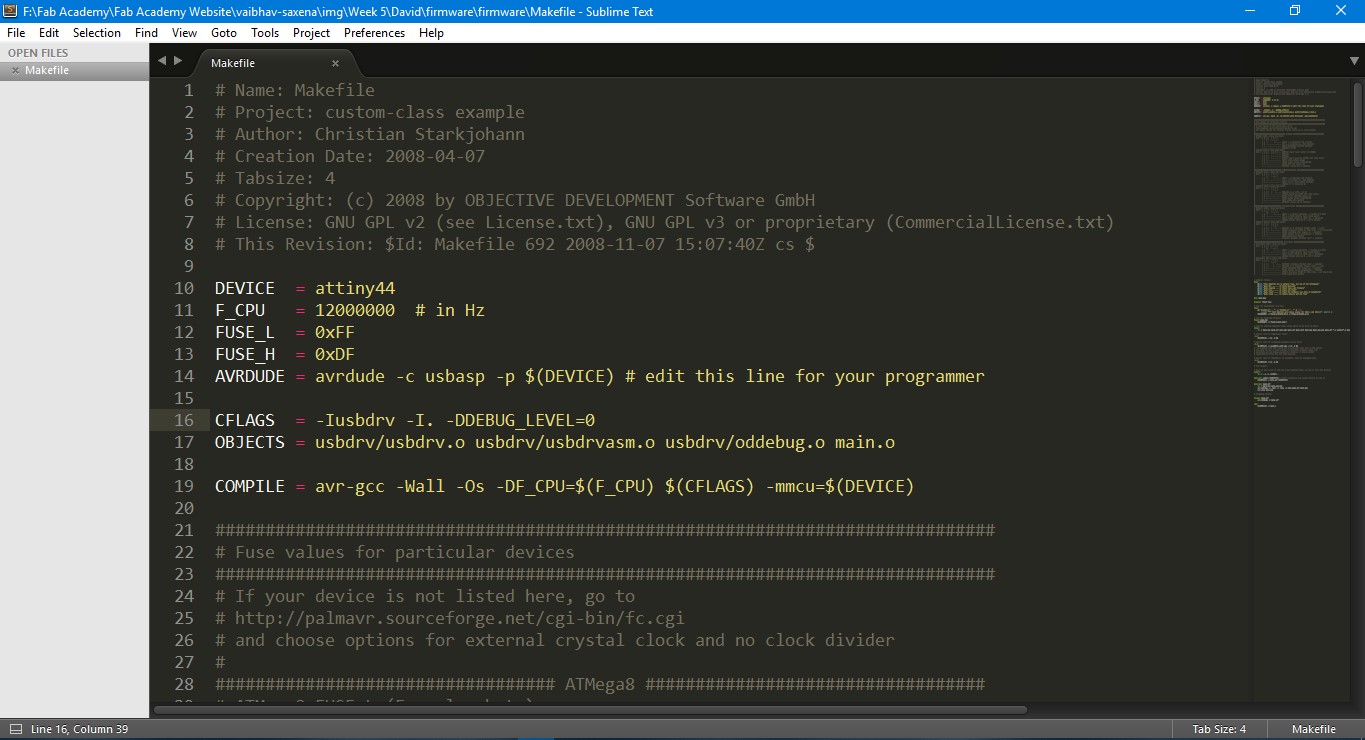
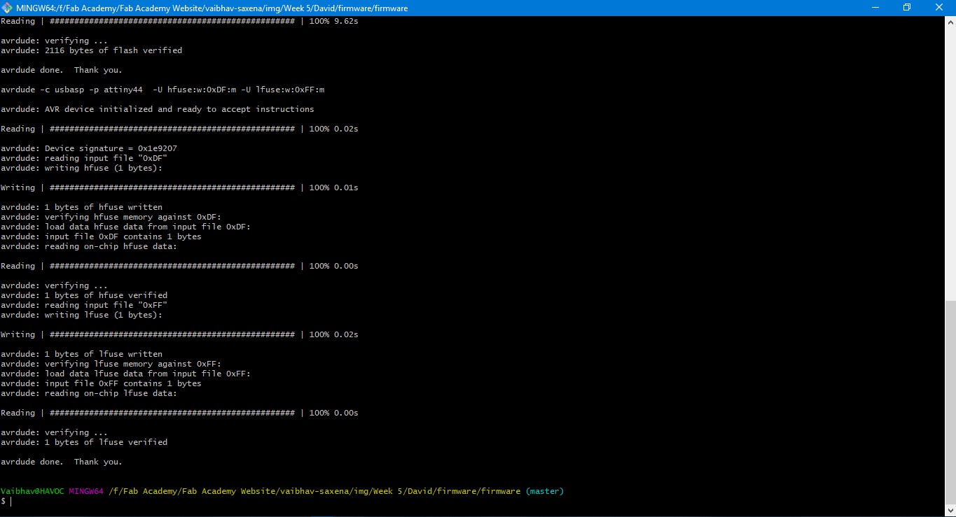
1. Since I was using USBasp, I had to edit David's Makefile from "avrdude -c usbtiny -p $(DEVICE)" to "avrdude -c usbasp -p $(DEVICE)"
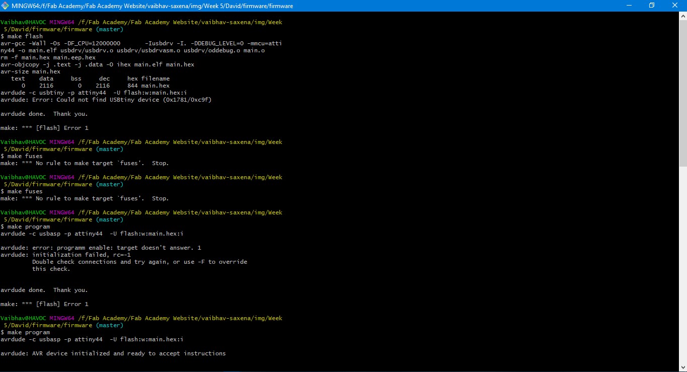
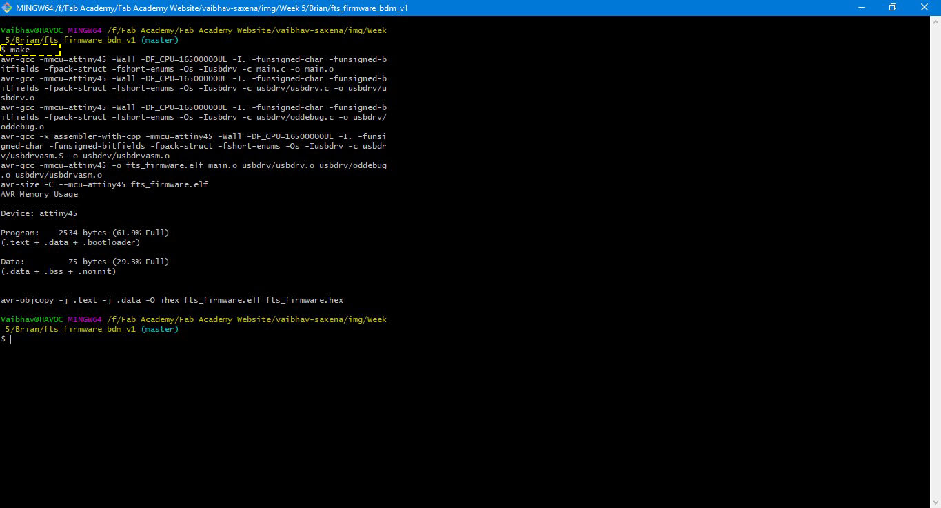
2. Once the above step has been performed, I opened the Git Bash in the David's firmware folder and executed the following programs(in the same order) a) make flash, b) make fuse and c)make program (even though make flash and make fuse didn't do anything as observed)
3. Make program command displayed that the FabISP has been programmed succesfully.
4. Now I had to disconnect the SJ1 jumper above the crystal.
After repeated attempts my computer couldn't detect the USBisp and hence I proceeded with Brian's board.
.jpg)
.jpg)
.jpg)